
The Packaging Bottleneck: Where AI Capex Actually Hits the Wall
Part 1 of 5 in The Bottleneck Map series: under-the-radar companies with asymmetric upside.

This is the first piece in a five-part series on where AI infrastructure capex is actually hitting walls and the under-the-radar names positioned to capture each one.
The premise of the series is that "AI infrastructure" is not one trade. It is at least five distinct bottlenecks (for now), each with its own physics, its own timing, and its own set of winners.
Most retail-focused commentary lumps these together and ends up either chasing the obvious large-cap names or buying generic "AI infrastructure" baskets. This series breaks the stack apart and identifies three to four under-the-radar players per bottleneck, names that genuinely capture the structural shortage rather than just trade on the narrative.
The five bottlenecks covered:
1. Packaging: TC bonding, hybrid bonding, glass substrates
2. Materials & Substrates: ABF, CMP, compound semiconductor epitaxy
3. The Memory Wall: CXL, disaggregated memory
4. Power & Thermal: liquid cooling, >100kW racks
5. Power Generation: behind-the-meter, gas turbines, nuclear, SMRs
Each piece stands alone and can be read independently, but the full picture is sequential: the further down the stack you go, the more under-priced the moats become and the further the names sit from mainstream coverage.
With that, let's get into the first one.
1. The Packaging Bottleneck
The first phase of AI capex was framed as a GPU supply story but that is no longer the full picture.
The constraint has moved one step downstream: advanced packaging. Making the GPU is no longer enough. Each Blackwell, Blackwell Ultra and Rubin module has to be packaged together with HBM memory at extremely high bandwidth.
The technology that does that is TSMC’s CoWoS (Chip-on-Wafer-on-Substrate). It’s the hard ceiling on how many modules actually ship.

Even with enough wafers, enough HBM and enough demand, shipments are limited by how much CoWoS capacity TSMC can provide.
UBS estimates Nvidia alone could demand 678,000 CoWoS wafers in 2026, around 40% above 2025. Morgan Stanley expects TSMC to reach 120,000 - 130,000 CoWoS wafers per month by end of 2026, up from 13,000 - 16,000 wafers per month in 2023. That is a massive capacity ramp and it still isn’t enough.
 | Seeking Alpha")
Apple, Qualcomm and Broadcom are reportedly struggling to secure slots. Apple has started recruiting engineers familiar with Intel’s EMIB technology (Embedded Multi-die Interconnect Bridge, Intel’s alternative to CoWoS that connects chiplets via small embedded silicon bridges instead of relying on a large interposer) as a hedge.
The packaging bottleneck has three sub-layers:
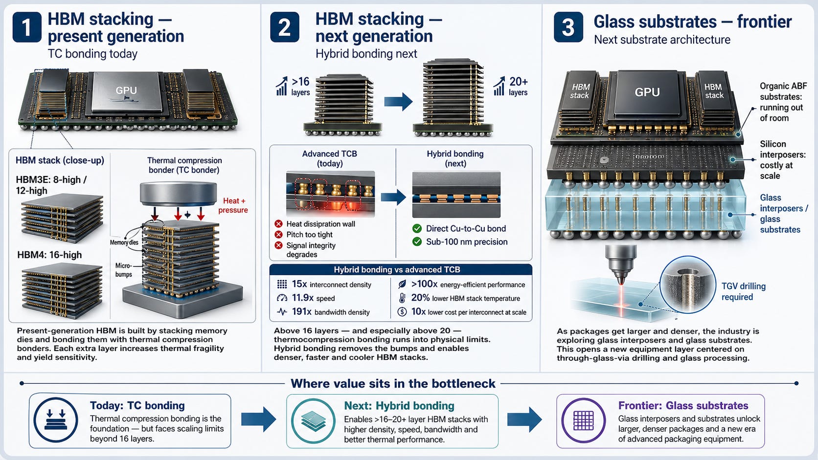
HBM stacking* (TC bonding today, hybrid bonding next),
The GPU-to-HBM interconnect (CoWoS-S, CoWoS-L, future glass interposers),
The substrate underneath.
*HBM stacking is the process of building the memory tower next to the GPU. Today that tower is mostly assembled using thermocompression (TC) bonding. In the future, the industry may move toward hybrid bonding to make the connections denser, faster and more efficient.
This piece looks at where the value sits inside that bottleneck and identifies three under-the-radar names positioned to capture different parts of it.
2. The TAM
Per Yole Group’s Status of the Advanced Packaging Industry 2025 report, the advanced packaging market grew 19% year-over-year in 2024 to $46B and is projected to exceed $79.4B by 2030, a 9.4% CAGR through 2030.
The fastest-growing segment is telecom and infrastructure (AI accelerators, GPUs, data center), forecast at 14.9% CAGR and that segment is the one drawing essentially all the incremental capex.
Inside advanced packaging, Yole tracks the back-end equipment market that supplies the bonding tools. Total back-end equipment revenue is estimated at $6.9B in 2025, growing to $9.2B by 2030 (5.8% CAGR).

Within that, the two pieces that matter for HBM and AI accelerators have very different trajectories:
TCB bonders: $542M (2025) → $936M (2030), 11.6% CAGR
Hybrid bonders: $152M (2025) → $397M (2030), 21.1% CAGR
Yole’s framing matters: TCB and hybrid bonding are among the fastest-growing back-end equipment segments through 2030.
Most retail-focused commentary lumps these together as if they were the same trade. They aren’t. They have different leaders, different timing, and different customer adoption curves.
The HBM supply backdrop is structurally tight. Per industry coverage of the most recent earnings calls, HBM supply is fully allocated through 2026, including HBM3E. Samsung has signaled high-teens to low-20% HBM contract pricing increases for 2026. CoWoS is oversubscribed through at least 2027.
The April 29, 2026 hyperscaler earnings round confirmed this dynamic in the most direct way possible. Meta raised 2026 capex guidance from $115-135B to $125-145B, a $10B increase at both ends of the range. The reason Meta gave in its 8-K filing is the data point that matters most for this piece:
“This reflects our expectations for higher component pricing this year and, to a lesser extent, additional data center costs to support future year capacity.”

Read the framing carefully. Meta is not buying meaningfully more units. It is paying meaningfully more per unit. The same dynamic showed up across the hyperscaler cohort:
Total 2026 capex guidance for the top five hyperscalers is now tracking toward $700-750B combined, up roughly 60-67% year-over-year, with components HBM, GPUs, advanced packaging, driving most of the increase.
This is the bullish translation of the bottleneck. When supply is constrained and demand is inelastic, prices do the work that volume can’t.
The customers buying HBM are passing the cost through. The companies making the equipment that produces that HBM, TC bonders, hybrid bonders, advanced packaging tools, are capturing the operating leverage of fixed-cost businesses selling into rising-prices end markets.
That is the structural setup behind the names covered in this piece.
3. Where the bottleneck splits
Three sub-bottlenecks make up the packaging stack, each binding at a different point in the technology curve:
HBM stacking, present generation. Memory dies bonded together using TC bonders (Thermal Compression Bonders). HBM3E uses 8-high or 12-high stacks; HBM4 introduces 16-high. Each layer makes the process more thermally fragile and yield-sensitive. TC bonders use heat and pressure to solder the dies through micro-bumps.
HBM stacking, next generation. Above 16 layers, and especially above 20, TC bonding hits physical limits. Heat dissipation becomes a wall, micro-bump pitch becomes too tight, and signal integrity degrades.
Hybrid bonding replaces the bumps entirely with direct copper-to-copper bonds at sub-100nm precision. Per Player 2 2025 Annual Report, hybrid bonding versus the most advanced TCB delivers 15x interconnect density, 11.9x speed, 191x bandwidth density, more than 100x energy-efficient performance, and reduces HBM stack temperature by 20%. Critically, it also delivers 10x lower cost per interconnect once volumes scale.
Glass substrates, frontier. As organic ABF substrates run into physical limits and silicon interposers become expensive at larger package sizes, the industry is exploring glass interposers and glass-core substrates.
But glass requires a new equipment layer. The key process is TGV formation, or through-glass-via drilling, which creates the vertical connections through the glass.
This is where LPKF becomes relevant. Its LIDE technology is designed to process glass with high precision and without microcracks, making it one of the key equipment plays on the glass substrate transition.
Per Yole's 2025 advanced IC substrate report, the total advanced substrate market reaches $31B by 2030, and within that, glass-core substrates are moving from nascent to commercial through 2026-2030.
The TGV equipment market that enables this transition is much smaller (under $1B) but growing at 21% CAGR through 2031, which is where Player 3 competes.
The timing of the transition from TC bonding to hybrid bonding is not fixed.
TC bonding is not disappearing tomorrow. In fact, recent industry updates suggest it may have a longer runway than expected.
According to TrendForce and Korean media reports, JEDEC reportedly relaxed the maximum HBM package height requirement from 775μm to around 900μm in early 2026. That matters because it gives memory makers more physical room to keep using existing TC bonding processes for taller HBM stacks.
SK Hynix is a good example. The company evaluated fluxless bonding for 16-high HBM4 in Q4 2025, but ultimately decided to stay with MR-MUF, suggesting that hybrid bonding is still too early for mainstream 16-high HBM production.
Samsung, however, is already pushing the next step. At Nvidia GTC 2026, Samsung demonstrated hybrid bonding and claimed more than 20% improvement in thermal resistance versus TC bonding.
The takeaway is simple:
TC bonding still owns the current HBM ramp, but hybrid bonding is becoming the next-generation technology to watch.
The investment logic is not “pick a packaging stock.” It is “understand which technology is binding now and who captures that flow.”
The three companies covered here capture three time horizons:
Present (TC bonding): Player 1
Near future (hybrid bonding): Player 2
Frontier (glass / TGV): Player 3
Each is exposed to the same macro driver, the structural advanced packaging shortage, but at different points in the curve.
